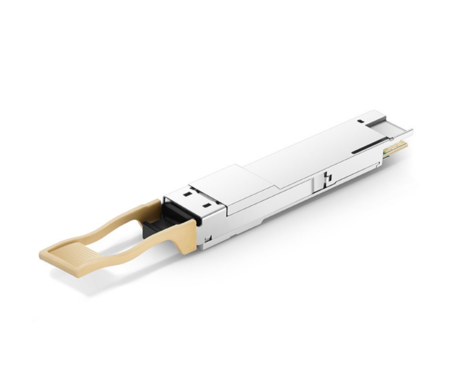
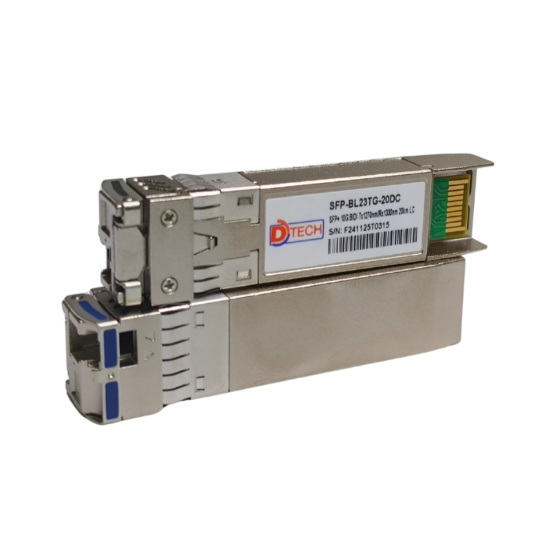
400G QSFP-DD SR8
Discover our latest products and services

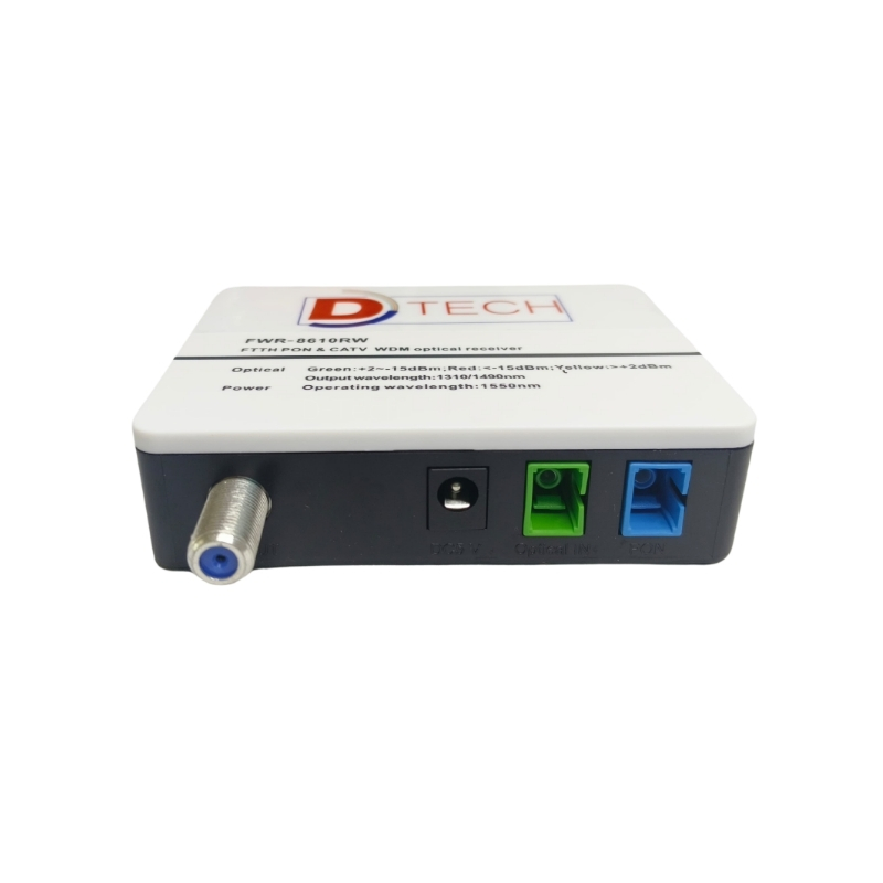
Available Variants
Product Info
- Brand: D-TECH
- Unit: pc(1)
- Product ID: 1256
Request a Quote
Contact us for pricing details.
Product Specifications
- Compatible: 288-TRIAL-Cisco, Juniper, Huawei, Nokia 106
- Warranty: 40-TRIAL-1 Year 242
400G QSFPDD SR8 Optical Transceiver
8 independent parallel optical channels
Each channel data rate up to 26.56GBaud with CDR
Hot Pluggable
Up to 100m link on OM4 Multi-mode
850nm VCSEL/PD Array Technology
CML Compatible electrical I/O
QSFP-DD MSA Compliance
Optical connectivity via industry standard MPO/MTPterminated fiber ribbon
MPO-16APCOpticalReceptacleType
CMIS 4.0 Compliance
Monitors for VCSEL bias, transmitted, received power , module temperature, and module supply
RoHS II Compliance
Case Operating Temperature:Commercial: 0 to 70oC
Applications
Highperformancecomputinginterconnect Datacenter
Description
QDD-MM85QG-SR8C is a QSFP-DD Optical transceiver for 8 x 26.56GBaud optical links. It is compliant with the QSFP-DD MSA specifications. It operates at 26.56GBaud up to 100m over OM4 Multi- mode fiber.
|
Parameter |
Symbol |
Min |
Max |
Units |
Notes |
|
Storage Ambient Temperature |
Tstg |
-40 |
+85 |
oC |
Exceeding the Absolute Maximum Ratings may cause irreversible damage to the device. The device is not intended to be operated under the condition of sim- ultaneous Absolute Maximum Ratings, a condition which may cause irreversible damage to the device. RH is Non- condensing condition. |
|
Relative Humidity - Storage |
RHS |
0 |
95 |
% |
|
|
Relative Humidity - Operating |
RHO |
0 |
85 |
% |
|
|
Module Supply Voltage |
VCC |
-0.5 |
3.6 |
V |
Recommended Operating Conditions
|
Parameter |
Symbol |
Min |
Typ |
Max |
Units |
Notes |
|
Case Operating Temperature |
Tcase |
0 |
+25 |
+70 |
oC |
Temperature Range = C |
|
Module Supply Voltage |
VCC |
3.14 |
3.3 |
3.46 |
V |
|
|
Power Consumption |
P |
10 |
W |
|||
|
Signaling Speed PerChannel |
S |
26.56 |
GBd |
Transmitter Electrical Interfaces
|
Parameter |
Symbol |
Min |
Typ |
Max |
Units |
Notes |
|
Tx_Data Differential Input Voltage |
VIN |
900 |
mV |
|||
|
Tx_Data Differential Input Impedance |
ZIN |
100 |
Q |
|||
|
Rx_Data Differential Output Voltage |
VOUT |
900 |
mV |
|||
|
Rx_Data Differential Output Impedance |
ZOUT |
100 |
Q |
|
Average Launch Power ,each lane |
POUT |
-6.5 |
4 |
dBm |
Average Optical Out-put |
|
|
Outer Optical Modulation Amplitude each lane |
OMAouter |
-4.5 |
3 |
dBm |
||
|
Optical Output with Tx OFF |
POFF |
-30 |
dBm |
|||
|
Extinction ratio |
ER |
3 |
dB |
|||
|
RMS Spectral Width |
Δλ |
0.6 |
nm |
|||
|
Transmitter and dispersion eye closure (TDECQ) each lane |
TDECQ |
4.5 |
dB |
|||
|
Launch power in OMAouter minus TDECQ, each lane (min) |
-5.9 |
dB |
||||
|
TDECQ – 10log10(Ceq), each lane (max) |
4.5 |
dB |
||||
|
RIN12 OMA |
RIN12 OMA |
-128 |
dB/Hz |
|||
|
Optical return loss tolerance (Max) |
ORLT |
12 |
dB |
Receiver Optical Characteristics
|
Parameter |
Symbol |
Min |
Typ |
Max |
Units |
Notes |
|
Center Wavelength |
λ |
840 |
850 |
860 |
nm |
|
|
Signaling rate, each lane |
SR |
26.56 |
GBd |
|||
|
Signaling Speed Accuracy |
-100 |
100 |
ppm |
|||
|
Modulation format |
PAM4 |
|||||
|
Average power at receive input, eachlane |
PIN |
-8.4 |
4 |
dBm |
Note1 |
|
|
Receive power (OMAouter), eachlane (max) |
3 |
dBm |
||||
|
Receiver sensitivity (OMAouter) eachlane |
Sen |
max(–6.6, SECQ – 8) |
dBm |
Note2 |
||
|
Rx_LOS of Signal - Assert |
PA |
-24.6 |
dBm |
|||
|
Rx_LOS of Signal - Deassert |
PD |
-7 |
dBm |
|||
|
Rx_LOS of Signal - Hysteresis |
PHy |
0.5 |
dB |
|||
|
Note 1: Average received power where the BER = 2.4E-4 measured with a PRBS 31Q test pattern@26.56GBaud Note 2: Sensitivity where the BER = 2.4E-4 measured with a PRBS 31Q test pattern@26.56GBaud |
||||||
Pin Description
|
Pin |
Symbol |
Description |
Notes |
|
1 |
GND |
Ground |
|
|
2 |
Tx2n |
Transmitter Inverted Data Input |
|
|
3 |
Tx2p |
Transmitter Non Inverted Data Input |
|
|
4 |
GND |
Ground |
|
|
5 |
Tx4n |
Transmitter Inverted Data Input |
|
|
6 |
Tx4p |
Transmitter Non Inverted Data Input |
|
|
7 |
GND |
Ground |
|
|
8 |
ModselL |
Module Select |
|
|
9 |
ResetL |
Module Reset |
|
|
10 |
VCC Rx |
Receiver +3.3V DC Power Supply |
|
|
11 |
SCL |
I2C Serial Clock |
|
|
12 |
SDA |
I2C Serial Data |
|
|
13 |
GND |
Ground |
|
|
14 |
Rx3p |
Receiver Non Inverted Differential Output |
|
|
15 |
Rx3n |
Receiver Inverted Differential Output |
|
|
16 |
GND |
Ground |
|
|
17 |
Rx1p |
Receiver Non Inverted Differential Output |
|
|
18 |
Rx1n |
Receiver Inverted Differential Output |
|
|
19 |
GND |
Ground |
|
|
20 |
GND |
Ground |
|
|
21 |
Rx2n |
Receiver Inverted Differential Output |
|
|
22 |
Rx2p |
Receiver Non Inverted Differential Output |
|
|
23 |
GND |
Ground |
|
|
24 |
Rx4n |
Receiver Inverted Differential Output |
|
|
25 |
Rx4p |
Receiver Non Inverted Differential Output |
|
|
26 |
GND |
Ground |
|
|
27 |
ModPrsL |
Module Present |
|
|
28 |
IntL |
Interrupt |
|
|
29 |
VCC Tx |
Transmitter +3.3V DC Power Supply |
|
|
30 |
VCC 1 |
+3.3V DC Power Supply |
|
|
31 |
Init Mode |
Initialization Mode |
|
|
32 |
GND |
Ground |
|
|
33 |
Tx3p |
Transmitter Non Inverted Data Input |
|
|
34 |
Tx3n |
Transmitter Inverted Data Input |
|
|
35 |
GND |
Ground |
|
|
36 |
Tx1p |
Transmitter Non Inverted Data Input |
|
|
37 |
Tx1n |
Transmitter Inverted Data Input |
|
|
38 |
GND |
Ground |
|
|
39 |
GND |
Ground |
|
|
40 |
Tx6n |
Transmitter Inverted Data Input |
|
41 |
Tx6p |
Transmitter Non Inverted Data Input |
|
|
42 |
GND |
Ground |
|
|
43 |
Tx8n |
Transmitter Inverted Data Input |
|
|
44 |
Tx8p |
Transmitter Non Inverted Data Input |
|
|
45 |
GND |
Ground |
|
|
46 |
Reserved |
No connect |
|
|
47 |
NC |
No connect |
|
|
48 |
VCC Rx1 |
+3.3V DC Power Supply |
|
|
49 |
NC |
No connect |
|
|
50 |
NC |
No connect |
|
|
51 |
GND |
Ground |
|
|
52 |
Rx7p |
Receiver Non Inverted Differential Output |
|
|
53 |
Rx7n |
Receiver Inverted Differential Output |
|
|
54 |
GND |
Ground |
|
|
55 |
Rx5p |
Receiver Non Inverted Differential Output |
|
|
56 |
Rx5n |
Receiver Inverted Differential Output |
|
|
57 |
GND |
Ground |
|
|
58 |
GND |
Ground |
|
|
59 |
Rx6n |
Receiver Inverted Differential Output |
|
|
60 |
Rx6p |
Receiver Non Inverted Differential Output |
|
|
61 |
GND |
Ground |
|
|
62 |
Rx8n |
Receiver Inverted Differential Output |
|
|
63 |
Rx8p |
Receiver Non Inverted Differential Output |
|
|
64 |
GND |
Ground |
|
|
65 |
NC |
No Connect |
|
|
66 |
Reserved |
No Connect |
|
|
67 |
VCCTx1 |
+3.3V DC Power Supply |
|
|
68 |
VCC2 |
+3.3V DC Power Supply |
|
|
69 |
Reserved |
No Connect |
|
|
70 |
GND |
Ground |
|
|
71 |
Tx7p |
Transmitter Non Inverted Data Input |
|
|
72 |
Tx7n |
Transmitter Inverted Data Input |
|
|
73 |
GND |
Ground |
|
|
74 |
Tx5p |
Transmitter Non Inverted Data Input |
|
|
75 |
Tx5n |
Transmitter Inverted Data Input |
|
|
76 |
GND |
Ground |


Additional Specifications
| Base Unit | pc(1) |
|---|---|
| Brand | D-TECH |
| Category | OFC Active Devices |
| SKU | |
| Product Code | 563 |
| Trackable | Yes |
| Taxable | Yes |
No videos available for this product.
.jpg)
Ratings & Reviews
Free Nationwide Delivery
Enjoy fast and free delivery across Nepal on all orders above Rs. 5,000. No hidden charges.
30-Day Hassle-Free Returns
Shop with confidence. Return or exchange your product within 30 days if you're not fully satisfied.
Up to 2 Years Warranty
All our products come with a standard warranty of up to 2 years, covering manufacturing defects.
No reviews yet. Be the first to review this product!
Login to leave a review.